
Thin-film transistor substrate including pixel regions where gate electrode lines are arrayed on an insulating substrate, and display therewith
US-7557373-B2Abstract
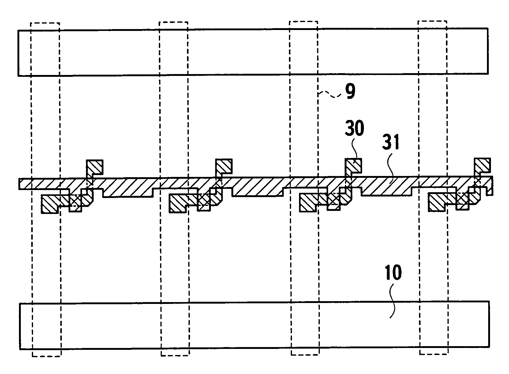
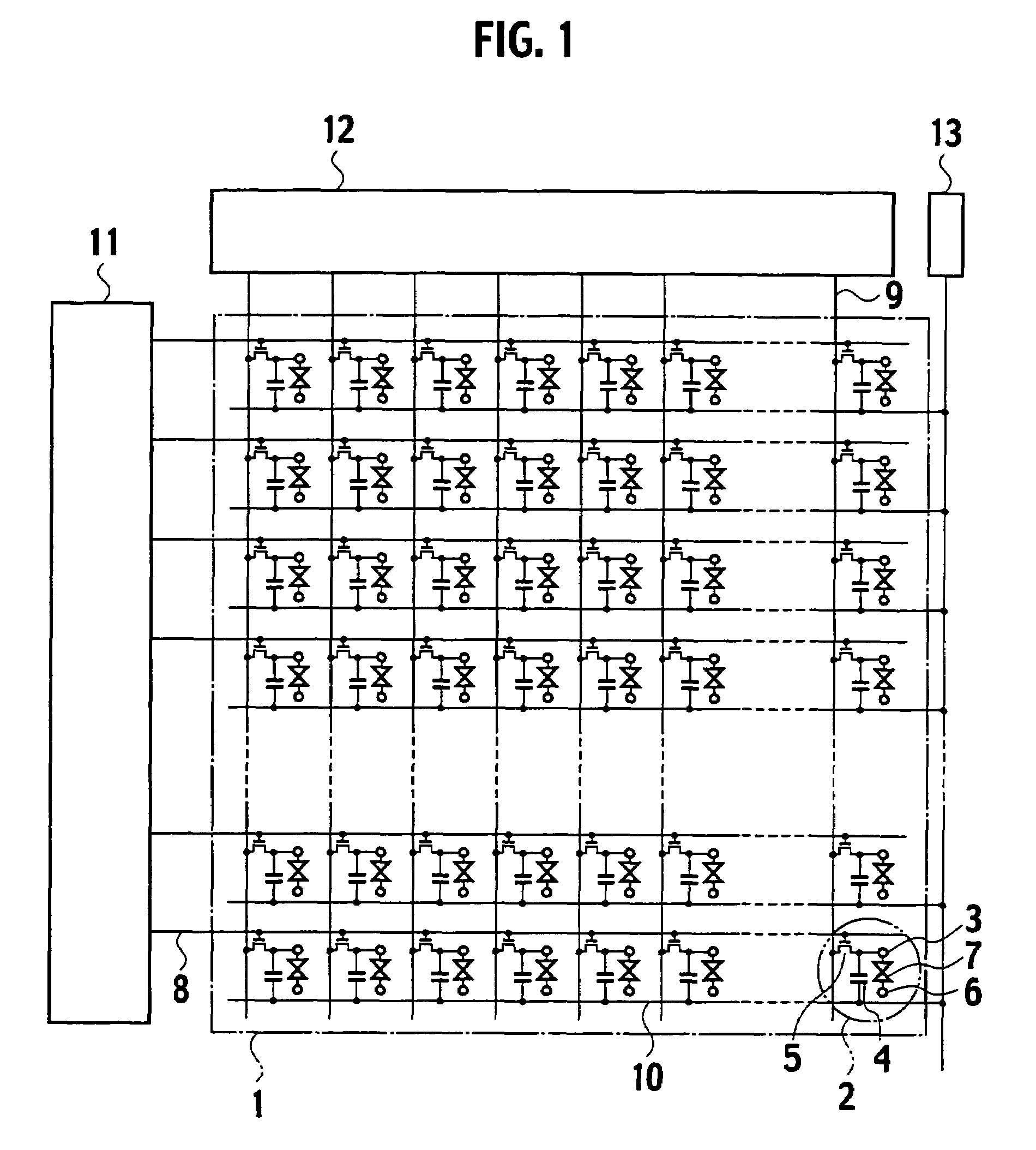
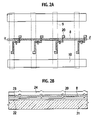
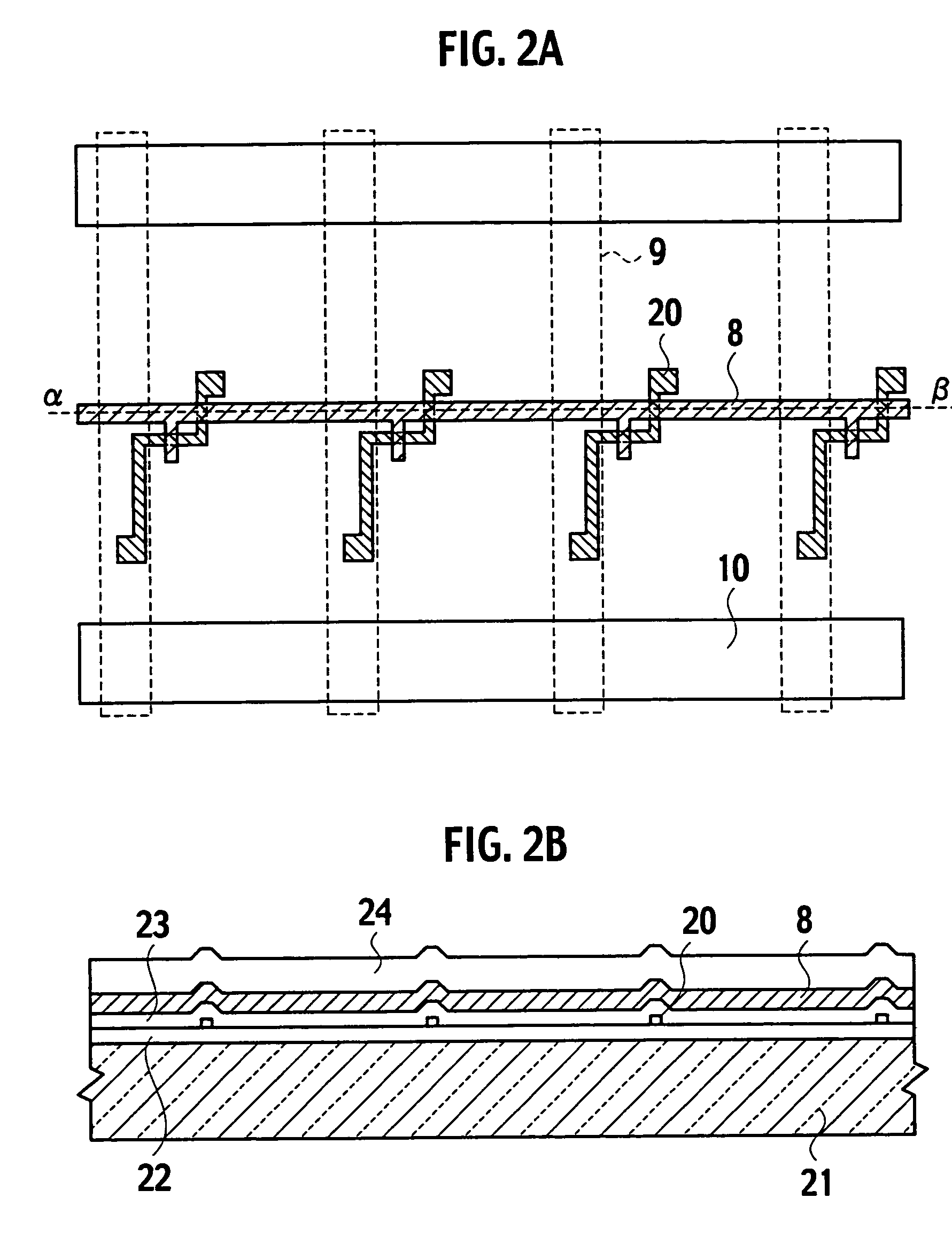
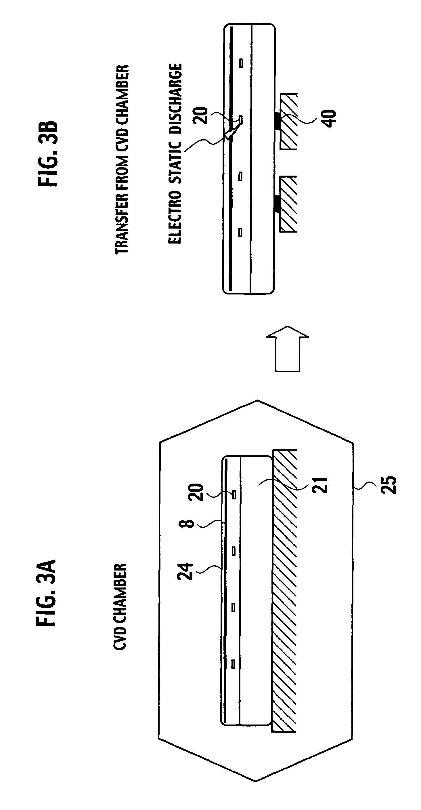
A thin-film transistor substrate includes a pixel region where gate electrode lines are arranged on an insulating substrate sandwiching semiconductor layer patterns and a gate insulator with the insulating substrate, wherein shapes of the semiconductor patterns and the gate electrode lines are set so that a value of K obtained by the following equation is smaller than a first set value when the thin-film transistor substrate is mounted on a metal table: K =( L/Ce )×{ Ca/ ( Ca+Cb )}× S where Ca represents a capacitor between each of the semiconductor layer patterns and the metal table, Cb represents a capacitor between each of the semiconductor layer patterns and the gate electrode lines, Ce represents a capacitor between each of the gate electrode lines and the metal table, L represents a length of each of the gate electrode line, and S represents a substrate surface area that one of the gate electrode lines are in charge of per unit length.
Patent figures(8)
Source status & events
No source-status events are recorded.