
来源记录显示 Expired
包括栅电极线排列在绝缘基板上的像素区域的薄膜晶体管基板以及具有该基板的显示器
Thin-film transistor substrate including pixel regions where gate electrode lines are arrayed on an insulating substrate, and display therewith
US-7557373-B2用于显示器,减少静电放电影响。
专利摘要
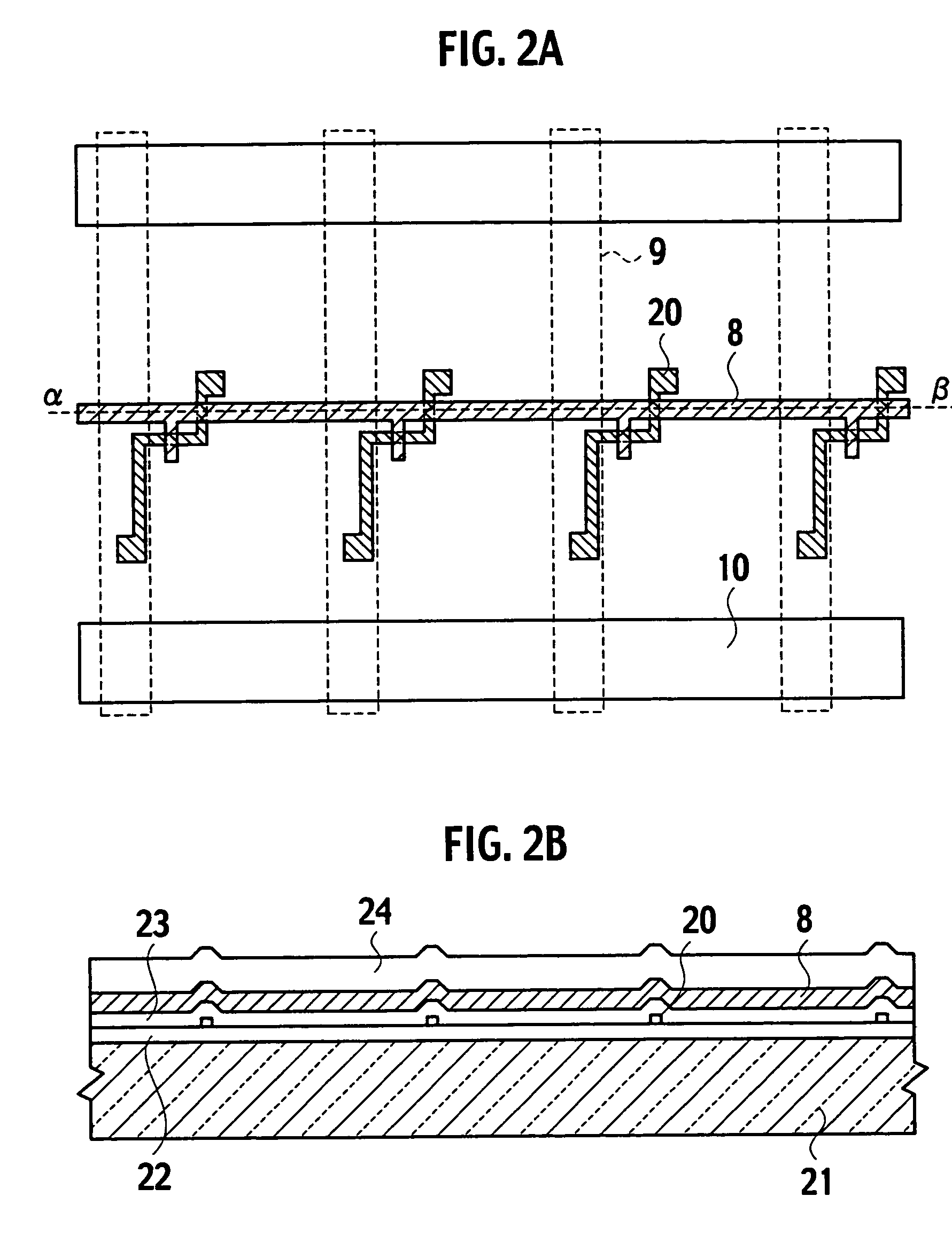
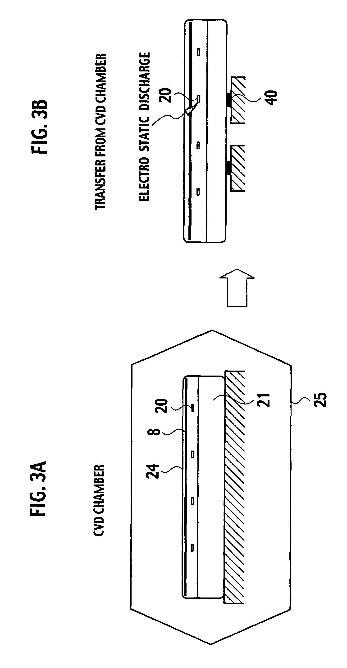
一种薄膜晶体管基板包括像素区域,其中栅电极线排列在绝缘基板上,半导体层图案和栅极绝缘体夹在绝缘基板之间,其中半导体图案和栅电极线的形状被设置为使得当薄膜晶体管基板安装在金属桌上时,由以下等式获得的K值小于第一设定值:K = (L/Ce) × {Ca/(Ca+Cb)} × S,其中Ca表示每个半导体层图案与金属桌之间的电容,Cb表示每个半导体层图案与栅电极线之间的电容,Ce表示每个栅电极线与金属桌之间的电容,L表示每个栅电极线的长度,S表示每个栅电极线每单位长度负责的基板表面积。
Original abstractA thin-film transistor substrate includes a pixel region where gate electrode lines are arranged on an insulating substrate sandwiching semiconductor layer patterns and a gate insulator with the insulating substrate, wherein shapes of the semiconductor patterns and the gate electrode lines are set so that a value of K obtained by the following equation is smaller than a first set value when the thin-film transistor substrate is mounted on a metal table: K =( L/Ce )×{ Ca/ ( Ca+Cb )}× S where Ca represents a capacitor between each of the semiconductor layer patterns and the metal table, Cb represents a capacitor between each of the semiconductor layer patterns and the gate electrode lines, Ce represents a capacitor between each of the gate electrode lines and the metal table, L represents a length of each of the gate electrode line, and S represents a substrate surface area that one of the gate electrode lines are in charge of per unit length.
专利附图(8)
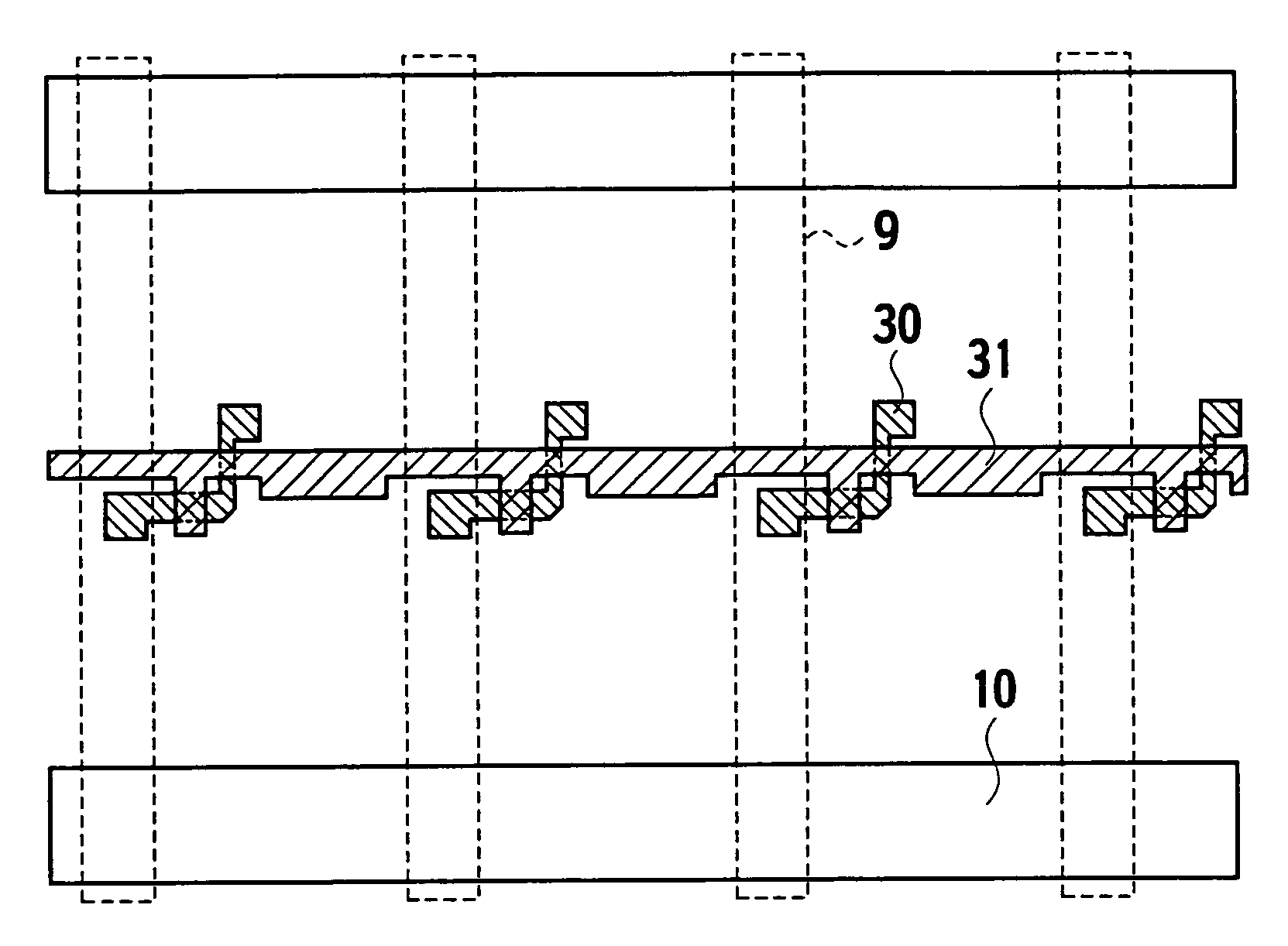
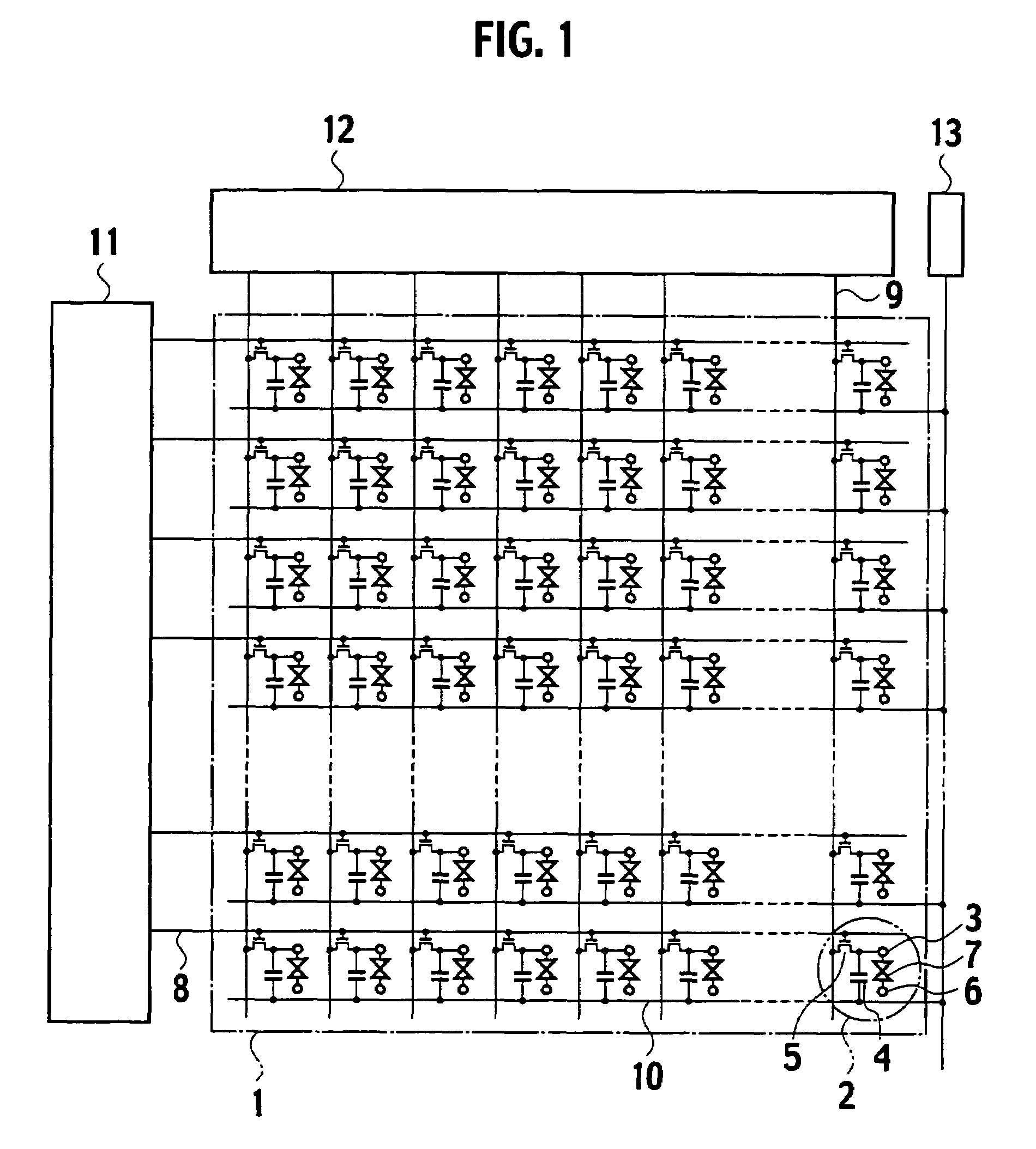
来源状态与事件
暂无可展示的状态事件记录。
相关专利(同品类)
使用须知
本页提供信息参考,不构成法律意见
来源状态不是法律结论专利状态可能因补缴、恢复、同族权利或地域差异而变化,应以当前权威记录和专业判断为准。
实施前应完成 FTO 评估任何生产、进口或销售决策前,应委托专利代理人或律师完成自由实施检索与侵权分析。