
来源记录显示 Expired
等离子体显示面板和等离子体显示装置
Plasma display panel and plasma display device
US-7482755-B2用于等离子体显示面板,提高驱动稳定性和显示性能。
专利摘要
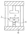
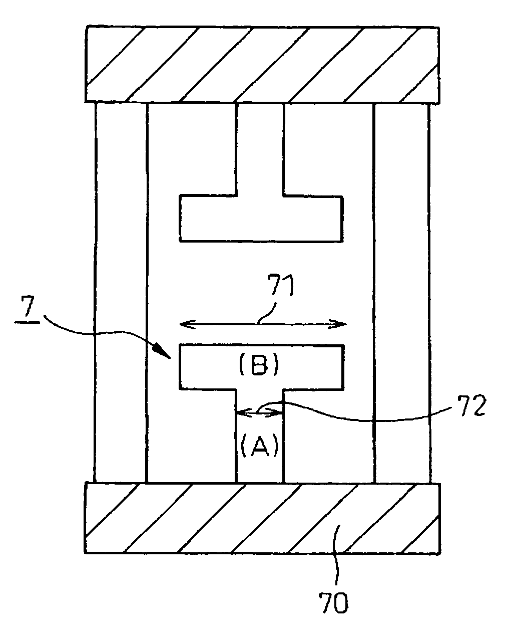
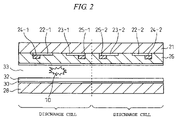
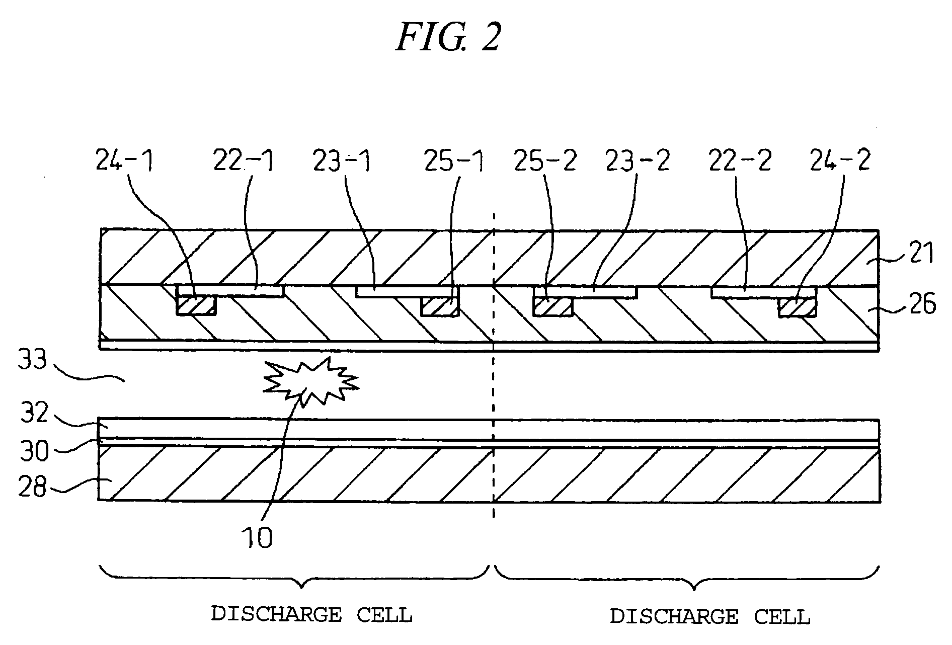
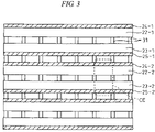
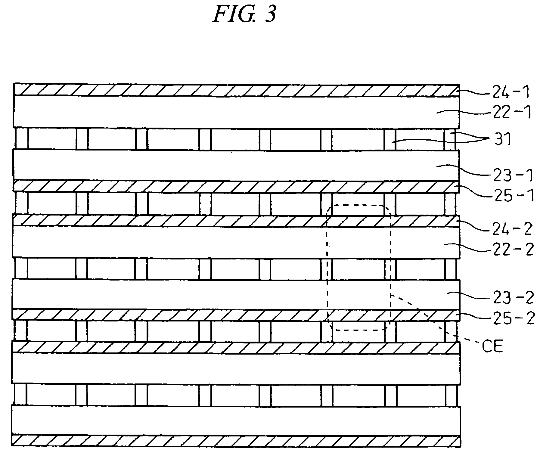
传统上,当在不改变电极形状的情况下减小介电层的厚度时,驱动裕度减小,无法进行稳定驱动。在放电单元中,显示电极包括从沿行方向延伸的电极主体沿列方向延伸的突起,该突起与另一显示电极的相邻配对突起一起形成放电间隙,该突起包括在行方向上具有两种宽度的第一突起和第二突起,并且当第二突起在放电间隙侧的宽度与第一突起在电极主体侧的宽度之比假定为Y,介电层的厚度假定为X时,满足Y≤0.2·X、X≤20和Y≥0.5。
Original abstractConventionally, when a thickness of a dielectric layer is reduced without changing an electrode shape, a drive margin is reduced and stable driving cannot be performed. In a discharge cell, a display electrode comprises a projection extending in a column direction from an electrode body extending in a row direction, the projection forms a discharge gap together with an adjacent paired projection of the other display electrode, the projection includes a first projection and a second projection having two kinds of widths in a row direction, and when a ratio of widths of the second projection on the discharge gap side to the first projection on the electrode body side is assumed as Y and a thickness of the dielectric layer as X, Y≦0.2·X, X≦20 and Y≧0.5 are satisfied.
专利附图(8)
来源状态与事件
暂无可展示的状态事件记录。
相关专利(同品类)
使用须知
本页提供信息参考,不构成法律意见
来源状态不是法律结论专利状态可能因补缴、恢复、同族权利或地域差异而变化,应以当前权威记录和专业判断为准。
实施前应完成 FTO 评估任何生产、进口或销售决策前,应委托专利代理人或律师完成自由实施检索与侵权分析。